


With the Union cabinet cleaning the planned support for multi-billion dollars to encourage semiconductor manufacturing in India, the spotlight once again on electronic components that are difficult to understand. The government launched a package worth 76,000 crore for local manufacturing to increase chip production that has paralyzed consumer electronics and the automotive industry.
Incentives must be offered to the company for six years and have been introduced to alleviate brands of misery of production deficiencies and secure the infrastructure of the country’s important information. This scheme is also expected to help establish India as a global center for consumer electronics, creating jobs and attracts investment from the Crore Rs 1.7 lakh.
The lack of chip that is currently highlighting the need to produce semiconductor chips locally, to meet the increasing demand and reduce the dependence of the state in imported chips, currently sourced mainly from China, Korea and Taiwan. Semiconductor chips, whose use is broad in several electronic items, computers and cars have caused the suspension of goods production throughout the industry, is expected to continue until the second quarter of next year, and it will likely cause further losses, especially for automotive. industry.
This scheme is expected to provide fiscal support which is needed, reducing tariffs on chip components, and has plans to set some great units. If you are wondering what the commotion is, here is the answer to a series of important questions about the topic.
What is the semiconductor fab unit?
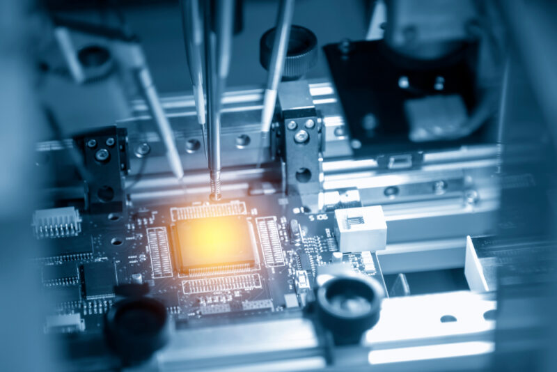
Fab semiconductors or fabrication factories, are basically a factory that produces integrated chip circuits and silicone wafers. Semiconductor chips are important components for all kinds of electronic goods and serve various functions such as powering displays, data transfer, etc. The manufacture of this chip is a complex process that takes more than three months and hence, with the right temperature requires controlled settings.
Each fab is responsible for producing semiconductor wafers that can vary in size. This wafer consists of several semiconductor chips which are then used to serve various industrial needs. While 300mm wafer foundries are more expensive, smaller requires a lower level of investment.
Given the rapid demand for consumer electronics, mixed with their reduced life span, many castings prefer to produce smaller wafers (100mm), which can be produced relatively fast. Regardless of the size of the unit is great, the cost always experiences tens of thousands of crores. Even though in the long run, more chips per wafer means a lower cost per chip for chip makers.
What happens in one?
The fabrication unit is needed to have a “clean room” where dust, vibration, temperature and moisture level are closely monitored because the existence of one of these factors can damage the entire product. According to an article in Forbes, the cleanest part of the FAB unit allows no more than 10 dust particles, size of about 10 microns per cubic meter air. Basically, even the specifications of microscopic dust can dispose of waste throughout the wafer.
Semiconductor fabrication units are some of the most sophisticated manufacturing units out there, which need thousands of ultra-high precision optics, lasers and advanced robotics to make hundreds of thousands of semiconductor wafers, each of which contains hundreds and thousands of semiconductor microchips. According to semi, the global industry association that represents the manufacturing and electronic design chain, the semiconductor manufacturing process can be broken down into five important parts.
Starting with a process called ‘deposition’ ‘where conductors and insulators are placed on silicon wafers. This is followed by patterns and etching, done, once again on the nano scale where the transistor pattern is placed to the wafer using a process called photolithography.
Materials that are widely categorized between conductors and insulators are then placed on silicon wafers after each component is measured and checked to ensure that hundreds of millions of components are basically defective. This is then followed by packaging involving building protective structures on the microcips and connection wafers of semiconductor wafers. Various types of semiconductors present different goals and can be found on hard disk drives, smartphones, televisions and cars, which last featured up to 50 to 150 semiconductors per car.
How much does it cost?
Semiconductor manufacturing equipment is very expensive and the Fab sophisticated unit is expected to cost around $ 15-20 billion. Even at the lower end, casting arrangements require capital intensive investment of $ 3-4 billion dollars or rs 22,000 crore. The equipment needed in the semiconductor fab unit also depreciates quite quickly.
In fact, according to Forbes, capital depreciation contributed 50-80 percent of this kind of plant manufacturing costs. Therefore the right type of tax subsidy is also needed for developing businesses. Labor training is also a factor, because the process of processing between 100mm to 300mm wafers requires a high level of skill, but especially tools and equipment that consens 80 percent.
Fab semiconductors also miss for a long time to be profitable, even though they have to overcome the industrial needs that are highly a discretion, especially to overcome the short life of consumer electronic goods. This is largely due to the high level of capital needed and the fact that semiconductor chips can depreciate up to 10 percent per year. For the type of chip it takes a car maker, the minimum capital required more than $ 4 billion, according to Bloomberg.
Where in India is being built?
At present, India has an ecosystem for making a beautiful embroidery semiconductor chip and imports 100 percent of its semiconductor. But India is a strong base for semiconductor chip designs. Chip design is a more severe process of software, and in accordance with the Electronic Ministry and Information Technology, India has a “fortress for chip design”.
Although semiconductor manufacturing has been in the pipeline for more than two decades, the infrastructure needed for the actual fabrication has been very inadequate. The creation of semiconductors involves design, manufacturing components and then fabrication. While the semiconductor design house has developed in India, and continues to do so, fabrication requires large investment and preferred tax subsidies that are not in India today.
It is contrast to countries such as the US, which offers $ 50 billion in investment subsidies. At present, India contributes to 20 percent of the semiconductor chip design capabilities, according to today’s business. The capital of IT India Bengaluru has several such design houses including Asm Technologies, Elxsi and Broadcom Inc., among others.
There is no one country that has a monopoly on semiconductor manufacturing, although China, Taiwan, USA, Japan and South Korea along with a handful of European countries, has a strong footing in this business. At present, some of the largest semiconductor casting includes Taiwan semiconductor manufacturing companies, which have become market leaders for several years, the second and global global global ones who have 10 fabrication factories worldwide (three in the US).
In the past several companies like that, including Intel had made proposals to the Government of India for the setting of great units, but nothing really materialized. Even the State-owned Hindustan Semiconductor Manufacturing Company does not take off, does not have documents required according to the intention letter, which is given by the government.